ASML, a Dutch company most people have never heard of, holds a major chokepoint in the modern chip economy. Without ASML EUV tools, manufacturers cannot produce leading-edge AI accelerators, smartphone processors, and data-center chips at frontier nodes. This single firm controls 100% of the extreme ultraviolet lithography market and approximately 83% of the global lithography market overall.[s] The implications span geopolitics, economics, and the future of artificial intelligence.
The Machine That Prints Everything
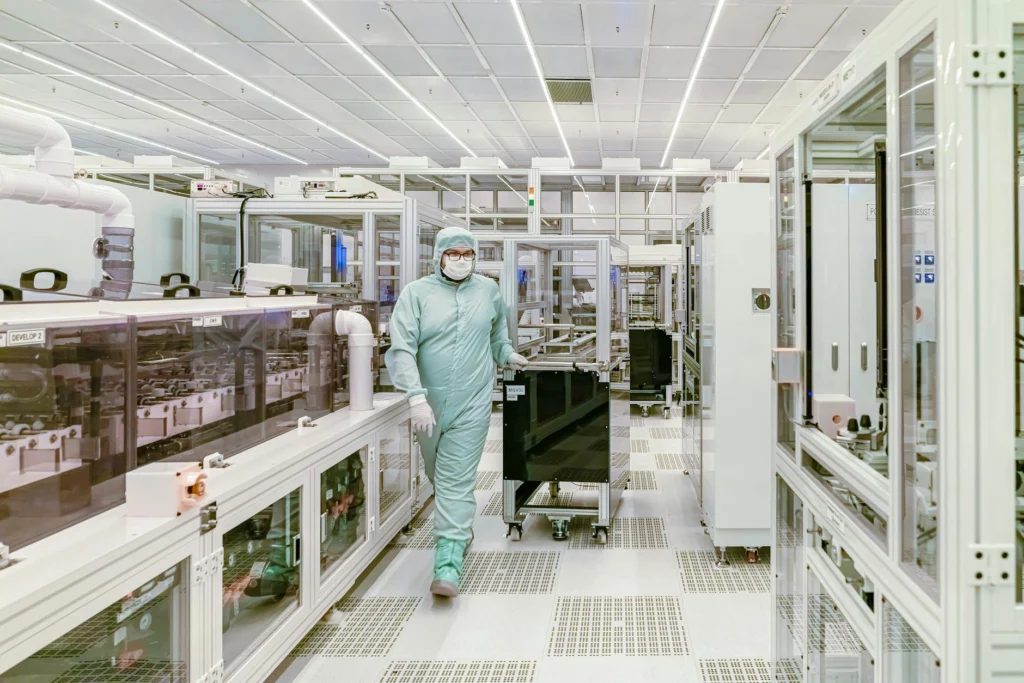
Leading-edge chips in volume production depend on ASML lithography machines. The company’s EUV systems are roughly the size of double-decker buses, contain over 100,000 components, and shipping one requires 40 freight containers, three cargo planes, and 20 trucks.[s]
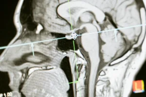
Lithography works by projecting light through a pattern onto a silicon wafer coated with photosensitive chemicals. Wherever light hits, the chemicals react, allowing engineers to etch microscopic circuits into the silicon. The shorter the wavelength of light, the smaller the features you can create. ASML’s EUV machines use light at 13.5 nanometers, thousands of times thinner than a human hair.
The physics are extreme. EUV light is absorbed by everything, including air, so the entire process happens in a vacuum. The light source works by hitting tiny droplets of molten tin with powerful lasers 50,000 times per second, creating plasma hotter than the surface of the sun. The mirrors required to focus this light must be polished to atomic-level smoothness.[s]
How This EUV Lithography Monopoly Formed
ASML’s dominance is not the result of market manipulation or superior business strategy alone. It emerged from decades of physics research, government investment, and strategic acquisitions.
Much of the foundational research came from the United States. Some of the most storied names in American R&D, including DARPA, Bell Labs, IBM Research, Intel, and the US National Laboratories, spent decades and hundreds of millions of dollars developing the technology that makes EUV possible.[s]
In 1997, a public-private partnership called the Extreme Ultraviolet Limited Liability Company formed to commercialize this research. ASML, initially barred as a foreign company, was eventually allowed to participate with conditions: establish a US research center and source 55% of components for US-sold systems from American suppliers.[s] In 2001, ASML acquired Silicon Valley Group, the sole American equipment manufacturer in the partnership, leaving ASML as the only surviving EUV developer.
Commercial EUV took more than two decades to reach production scale after decades of public-private research.[s] No competitor has replicated that full ecosystem.
The Supplier Web
ASML does not build EUV machines alone. Its system depends on exclusive partnerships with specialized suppliers that took decades to develop.
Carl Zeiss SMT provides the optical systems: mirrors polished to atomic-level precision, where an imperfection across a Germany-sized surface would measure in millimeters. The optical system in a High-NA EUV machine contains around 65,000 parts and takes a year to produce. Developing this system took over 10 million working hours and 25 years of collaboration with ASML.[s]
ASML invested €1.5 billion in Carl Zeiss SMT and acquired a 24.9% stake in 2016. Without Zeiss, ASML operations would halt completely.[s]
Cymer, which ASML acquired in 2013, provides the light source technology. TRUMPF supplies the CO2 lasers. VDL builds the wafer handling systems. This interdependence is the EUV lithography monopoly’s foundation: even if you somehow built a competing machine, you would need to recreate an entire global supply chain.
Why No One Can Compete
China has invested heavily in developing domestic lithography. Shanghai Micro Electronics Equipment (SMEE) has developed tools for mature nodes and has been trying to introduce 65nm- and 28nm-grade systems, but adoption remains limited. Local lithography tools remain a critical gap: most Chinese production lines still use ASML or Nikon machines, even older models.[s]
SMIC, China’s leading chipmaker, has demonstrated 7nm production using older DUV equipment through a technique called multi-patterning, where each layer requires three or four separate exposures instead of one EUV pass. EUV lithography can combine three or four patterning cycles into a single one; without it, producing 5nm nodes might require as many as 100 different steps.[s]
The results show the cost: SMIC’s 7nm yield is estimated at 20-40% compared to TSMC’s 80%+ at the same node. Per-chip cost runs roughly 50% above TSMC’s EUV-based equivalent.[s]
Huawei attempted to hire engineers from Zeiss SMT in late 2024, reportedly offering salaries up to three times higher.[s] Even aggressive talent poaching has not closed the gap. Public estimates for a production-capable Chinese EUV tool vary widely, with optimistic open-source assessments around 2030 and more cautious Western estimates often in the 2032-2035 range.[s]
Japan’s Rapidus, backed by government funding and IBM technology, hopes to achieve leading-edge production by 2027. But countries that industrialized in four decades during the Meiji era faced simpler physics. Semiconductor manufacturing at the frontier involves precision measured in atoms, and the industry has seen major players with enormous resources, including IBM, Motorola, and Texas Instruments, fail to stay competitive.[s]
The Business of Monopoly
ASML’s Q1 2026 results illustrate the scale: €8.8 billion in revenue, 53% gross margin, €2.8 billion net income in a single quarter.[s] Full-year 2026 guidance sits at €36-40 billion.
Each production-capable High-NA EUV system (the EXE:5200B) weighs 150,000 kilograms, requires 250 shipping crates, takes six months and 250 engineers to assemble on-site, and costs approximately $380 million.[s]
The EUV lithography monopoly extends beyond new machine sales. ASML’s installed-base management sales were €2.49 billion in Q1 2026, up from €2.13 billion in Q4 2025.[s] ASML does not just sell you the tool; it sells you every upgrade, every service contract, every software key that improves throughput.
Memory manufacturers are now diversifying ASML’s customer base. SK Hynix procured roughly 30 EUV machines in early 2026, paying premium prices for expedited delivery, while Samsung accelerates purchases for 1c DRAM.[s] This weakens TSMC’s bargaining power and strengthens ASML’s position.
What This Means
The EUV lithography monopoly is not a market distortion waiting to be corrected. It is a physics constraint that no amount of money or policy can quickly overcome. The technology took decades of coordinated R&D across multiple countries to develop. The supply chain spans Germany, the Netherlands, Japan, and the United States, with exclusive partnerships cemented by decades of co-development and equity stakes.
Export controls have blocked Chinese access to EUV since 2019, and restrictions now extend to advanced DUV immersion systems as well. Chinese customers purchased an estimated 70% of ASML’s DUV immersion systems in 2024, stockpiling ahead of tighter restrictions.[s]
Leading-edge AI accelerators depend on chips made with ASML lithography. ASML holds all the cards, possessing a 100% absolute monopoly on EUV lithography machines used for leading-edge chip manufacturing.[s] For better or worse, a consequential industrial chokepoint sits in a small Dutch city most people cannot pronounce.
EUV Physics and System Architecture
ASML’s NXE and EXE platforms generate 13.5nm wavelength light through laser-produced plasma. A CO2 laser (TRUMPF) pre-pulses molten tin droplets to flatten them, then a main pulse vaporizes the tin at roughly 50,000 pulses per second, creating plasma that emits EUV radiation. The source must sustain 250W+ continuous power for production throughput; reported Chinese prototype sources remain below that level, and no working chip from a domestic Chinese EUV tool has been publicly verified.[s]
EUV light is absorbed by all solid materials and air, necessitating a full vacuum optical path and reflective optics rather than transmissive lenses. The Zeiss SMT mirror stack uses multilayer Mo/Si coatings with approximately 70% reflectivity per surface. With multiple reflections through the illuminator and projection optics, total light throughput is roughly 2-4%. Mirrors must maintain sub-angstrom surface roughness across meter-scale surfaces.[s]
At 0.33 NA (low-NA EUV), the NXE:3800E achieves 13nm single-exposure resolution at 195-230 wafers per hour with sub-1.1nm matched-machine overlay. The EXE:5200B High-NA platform operates at 0.55 NA, shrinking minimum resolution to 8nm and enabling approximately 2.9x transistor density improvement in a single exposure. Each EXE:5200B weighs 150,000kg and requires 250 shipping crates.[s]
The Architecture of the EUV Lithography Monopoly
The monopoly rests on three pillars: exclusive supplier relationships, accumulated process knowledge, and network effects across the semiconductor ecosystem.
Zeiss SMT’s optical system represents 25+ years of co-development. The High-NA optical module contains 65,000 parts, weighs 3.5 tons, and takes one year to manufacture. Development required 10 million+ working hours.[s] ASML holds 24.9% equity in Zeiss SMT, with €1.5 billion invested since 2016. Cymer’s laser-produced plasma source, acquired in 2013, brought key EUV light-source technology inside ASML. TRUMPF provides the seed CO2 lasers. VDL builds wafer stages achieving sub-nanometer positioning accuracy with 20,000 adjustments per second.
The supplier ecosystem is geographically distributed and interdependent. No single country controls all components. Replicating the EUV lithography monopoly would require simultaneously developing: precision optics at the Zeiss level, high-power laser systems, vacuum-compatible wafer handling, computational lithography software (ASML’s Brion subsidiary), and decades of yield optimization data from customer fabs.
Some of the most storied names in US R&D, including DARPA, Bell Labs, IBM Research, Intel, and the US National Laboratories, spent decades of research and hundreds of millions of dollars to make EUV possible.[s] ASML’s 2001 acquisition of Silicon Valley Group consolidated all this IP under one roof.
DUV Multi-Patterning and Its Limits
Without EUV, manufacturers use DUV immersion (193nm wavelength, 1.35 NA) with multi-patterning: self-aligned double patterning (SADP), self-aligned quadruple patterning (SAQP), or litho-etch-litho-etch sequences. EUV lithography can combine three or four patterning cycles into a single exposure at 7nm. Without EUV, producing 5nm nodes might require as many as 100 different steps.[s]
SMIC’s N+2 process (7nm-equivalent) uses SAQP with four lithography passes per critical layer. Reported yields: 20-40% vs TSMC’s 80%+ at N7. Per-wafer cost approximately 50% higher than EUV-based equivalent.[s]
Multi-patterning compounds defect probability with each additional exposure, multiplies cycle time, and requires extremely tight overlay between passes. It is a viable workaround for sovereign demand insensitive to cost, not a competitive manufacturing strategy.
Challenger Technologies
Canon’s FPA-1200NZ2C nanoimprint lithography (NIL) represents the only alternative patterning approach with production capability. NIL uses direct mechanical pattern transfer rather than optical exposure: a template physically contacts the resist to stamp patterns. Specifications: 80-100 wafers per hour (vs 195+ for low-NA EUV), 14nm minimum linewidth, 2.4-3.2nm overlay (vs sub-1.1nm for EUV).[s]
NIL’s defect density from template-resist contact makes it unsuitable for leading-edge logic, where single-particle contamination kills entire dies. Its niche remains high-layer-count 3D NAND with forgiving overlay tolerances. No major foundry has committed to NIL for high-volume logic.[s]
Chinese efforts include Huawei-backed SiCarrier, Shanghai Yuliangsheng, and SMEE. SMEE has 90nm DUV tools in production and has been reported to have 28nm-grade immersion systems in late development, far behind ASML’s EUV tools. Public reports have described Chinese EUV light-source prototypes, but no working chip has been produced with a domestic EUV system.[s]
Open-source estimates vary: optimistic assessments put a production-capable Chinese EUV tool around 2030, while more cautious Western estimates often point to 2032-2035.[s] Even optimistic timelines assume no further export control escalation on precursor equipment, specialty gases, or metrology tools.
ASML Roadmap: Low-NA, High-NA, Hyper-NA
ASML’s roadmap spans four generations. DUV immersion (NXT series) remains the backbone for non-critical layers: 131 systems shipped in 2025. Low-NA EUV (NXE series, 0.33 NA) enabled 5nm/3nm nodes: 48 systems shipped in 2025. The NXE:3800F targets ≥260 wafers per hour and ≤0.9nm overlay by 2027-2028; NXE:4200G targets ≥300 wafers per hour by 2030-2031.[s]
High-NA (EXE series, 0.55 NA) entered early production in 2025. Intel completed acceptance testing of its EXE:5200B in December 2025 for 14A node development. SK Hynix installed the first memory-sector High-NA system at M16 fab. The EXE:5200B delivers 175 wafers per hour at 50mJ/cm² dose with 0.7nm overlay. Price: approximately $380 million.[s]
TSMC has publicly stated it will not adopt High-NA for A16 or A14, while analysts cited by Tom’s Hardware expect adoption around A10 (~2029-2030).[s] This reflects confidence that ASML’s installed-base upgrades can push 0.33 NA further than originally projected.
Hyper-NA (0.75 NA target, 0.85 NA under investigation) appeared on ASML’s roadmap in May 2024. Estimated tool cost: approximately $720 million. Technical barriers include polarization-induced contrast loss at extreme angles, depth-of-focus degradation, and an electron blur limit of approximately 2nm that may impose a hard resolution floor regardless of optical improvements.[s]
Economics of the EUV Lithography Monopoly
ASML Q1 2026: €8.8 billion revenue, 53.0% gross margin, €2.8 billion net income. Full-year 2026 guidance: €36-40 billion revenue, 51-53% gross margin.[s]
ASML reported €2.49 billion in installed-base management sales in Q1 2026, up from €2.13 billion in Q4 2025.[s] This recurring revenue stream from upgrades, maintenance, and software licenses provides downside protection independent of new tool sales.
Customer concentration is counter-intuitively a strength rather than weakness in this context. TSMC is one of ASML’s most important customers, but the dependence cuts both ways: leading-edge fabs build process recipes, yield data, mask flows, and process development kits around ASML tool characteristics. The ecosystem has converged around ASML as a central standard for EUV production.
Memory manufacturers are diversifying ASML’s revenue base. SK Hynix procured roughly 30 EUV machines in early 2026, willingly paying premium for expedited delivery, while Samsung accelerates purchases for 1c DRAM.[s] This customer diversification strengthens ASML’s pricing power relative to any single buyer.
Geopolitical Implications
EUV export controls have blocked Chinese access since 2019. Dutch restrictions expanded to advanced DUV immersion (NXT:2000i and newer) in late 2023, and to NXT:1970i/1980i by September 2024. Service restrictions prohibit ASML from improving overlay accuracy or increasing throughput by more than 1% on installed Chinese systems.[s]
Chinese stockpiling was substantial: an estimated 70% of ASML’s DUV immersion systems went to Chinese customers in 2024, front-loading purchases before restrictions tightened.[s] This provides a finite runway for DUV-based production at SMIC and others, but no path to EUV.
Japan’s Rapidus, with $15 billion in government backing and IBM technology transfer, targets 2027 mass production. History offers perspective: countries that industrialized in four decades during earlier eras faced simpler physics. Leading-edge semiconductor manufacturing involves atomic-scale precision, and even well-funded attempts by major corporations have failed. IBM, Motorola, and Texas Instruments all exited leading-edge manufacturing despite enormous resources and decades of experience.[s]
The EUV lithography monopoly has become a strategic chokepoint because the physics of light at 13.5nm wavelength, the precision of atomic-scale optics, and the coordination of a global supply chain built over decades cannot be replicated by policy alone. ASML holds a 100% absolute monopoly on EUV lithography machines used for leading-edge chip manufacturing.[s] For the foreseeable future, controlling access to these machines means shaping access to leading-edge AI compute.